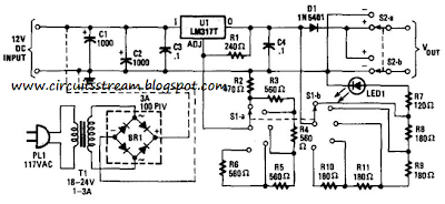
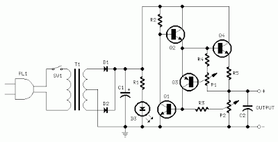
Solid State Relay - Required Only 50uA Drive Current

This circuit demands a control current that is 100 times smaller than that needed by a typical optically isolated solid state relays. It is ideal for battery-powered systems. Using a combination of a high current TRIAC and a very sensitive low current SCR, the circuit can control about 600 watts of power to load while providing full isolation and transient protection.

Sourced by :link

Simple Electronic Quiz Switch

One of the common  rounds in the  quizzes is the buzzer round. We are describing here a simple electronic circuit that can be used in any test or quiz competition. In this circuit, only four persons can participate,  and  every  participant is assigned a certain number. Whenever a switch is pressed, the circuit locks the remaining three entries. At the same time, an alarm sounds and the designated switch number is displayed on the seven segment LED display.When a player presses his switch, the corresponding output of IC1 goes high. Let us suppose, when switch S1 is pressed, D1 input of IC1 goes low and its corresponding output Q1 goes high. As a result, current passes through D5 to piezo buzzer PZ1, which creates a beep. At the same time, current also passes through diodes D6-D7 to show the number on the LED display.

Simple Electronic Quiz Switch Circuit diagram:

Simple Electronic Quiz Switch Circuit Diagram

Similarly, when any other switch (S2-S4) is pressed, the corresponding  number  gets  displayed  on  seven segment displaying DIS1 and buzzer sounds. Switch S5 is used to reset the display exclusively. Switch S5 is a push to on switch. The circuit is powered by 9V battery. Assemble the circuit on a general purpose PCB and enclose it in a suitable  case along with seven segment display and piezo buzzer. The assembled circuit can be kept near the host and the switches connected through the external can be assigned to the players. 

Author : Siddeeq Basha  - Copyright : EfyMag

Analog to Digital Converter Circuit Diagram

This is a digital Analog to Digital Converter Circuit Diagram. Perhaps the most important consideration of an ADC is its resolution. Because the CS5501 16-bit-delta-sigma analog-to-digital converter lacks a start convert command, it converts continuously, outputting conversion words to its output register every 1024 cycles of its master clock. However, by incorporating a standard dual J-K flip-flop into the circuit, the ADC can be configured to output a single-conversion word only when it is polled.

 Analog to Digital Converter Circuit Diagram


Analog to Digital Converter Circuit Diagram


The CS5501 converter can be operated in its asynchronous communication mode (UART) to transmit one 16-bit conversion word when it is polled over an RS-232 serial line (see figure). A null character (all zeros) is transmitted to the circuit and sets the flip-flop PF2. The CS5501 can then output a single-conversion word, which is transmitted over the RS-232 line as two bytes with start and stop bits.

The baud rate can be chosen by selecting the appropriate clock divider rate on the 74HC4040 counter/divider as the serial port clock (SLCK) for the ADC. This type of polled-mode operation is also useful when the ADC`s output register is configured to operate in the synchronous-serial clock (SSC) mode. In this case, the converter will load one output word into a 16-bit serial-to-parallel register (two 74HC595 8-bit registers) when polled to do so (see figure).

Simple Analog-to-Digital Converter with LT1018

This is a Simple Analog-to-Digital Converter with LT1018. An analog-to-digital converter (abbreviated ADC, A/D or A to D) is a device that converts a continuous physical quantity (usually voltage) to a digital number that represents the quantity's amplitude.The converter has a 60-ms conversion consumes 460 pA of 1's. 5 V power supply and maintains an accuracy of 10 bits on a 15 ° C in the temperature range of 35 ° C. 

 Simple Analog-to-Digital Converter with LT1018 Circuit Diagram


Simple Analog-to-Digital Converter with LT1018 Circuit Diagram


A pulse applied to convert the command line causes Q3, operating in reverse mode, the discharge path through the diode 10 kO, forcing its collector low. Q3 results of reverse mode switching in a capacitor discharge to 1 mV of ground. During the time of the ramp value is less than the input voltage, output of the CIA is low. 

This allows pulses ClB stabilized quartz oscillator, modulating Q4. The output data appears at the collector of Q4. When the ramp crosses the starting value of the output voltages of the CIA is going up, Q4 polarization and output data continuously. The number of pulses at the output is directly proportional to the input voltage. To celebrate cali apply 0.5V to the input and the TRIM-10 kO exactly 1000 pulses each time the conversion from the command line is pulsed.

Solar Powered Animal Scarer

Here is a solar powered Flasher to scare away the nocturnal animals like bats and cats from the farm yard or premises of the house. The brilliant multicolored flashes confuse these animals and they avoid the hostile situation. It is fully automatic, turns on in the evening and turns off in the morning.

The circuit has an LDR controlled oscillator built around the Binary counter IC CD 4060.The functioning of the IC is controlled through its reset pin 12. During day time, LDR conducts and keeps the reset pin of IC high so that it remains dormant. During night, LDR cease to conduct and the reset pin will be grounded through VR1. This triggers the IC and it stats oscillating using the components C1 and VR2. Output pins 7, 5 and 4 are used to power the LEDs strings.

VR1 adjusts the sensitivity of LDR and VR2, the flashing rate of LEDs. High bright Red, Blue and White LEDs are used in the circuit to give brilliant flashes. Red LEDs flash very fast, followed by blue and then White. White LEDs remains on for few seconds and provide light to a confined area. More LEDs can be added in the strings if desired. The circuit can also function with 12 volt DC.

Animal Repellent Circuit Diagram

Circuit Project: Solar Powered Animal Scarer

The circuit uses a solar powered battery power supply. During daytime, battery charges through R1 and D1.Green LED indicates the charging mode. During night time current from the solar cell decreases and D1 reverse biases. At the same time D2 forward biases to provide power to the circuit. Resistor R1 restricts the charging current and the high value capacitor C1 is a buffer for current.

Animal Scarer Solar Power Supply

Circuit Project: Solar Powered Animal Scarer

Two-Zone Burglar Alarm

Descrition


This is a two-zone alarm - with automatic exit, entry and siren cut-off timers. It can be triggered by the usual types of normally-closed input devices - such as magnetic reed contacts - foil tape - PIRs etc. I've used a 12-volt supply in the diagram - but the circuit will work at anything from 9 to 15-volts. All you need do is select a siren, buzzer and relay to suit the voltage you want to use.

Schematic Diagram


When you move Sw1 to the Set position - you have about 30 seconds to leave the building. If you re-enter through the Exit/Entry zone - the buzzer will sound - and you'll have about 30 seconds to switch the alarm off. The Instant zone has no entry delay. Anyone entering through the Instant zone - will sound the siren immediately.

About ten minutes after the normally-closed loops have been restored - the siren will switch off - and the alarm will return to standby mode. It can then be re-activated by a subsequent intruder. If you don't want the siren to sound a second time - add the One-Time-Only Module. It forces the siren to switch off after the first ten minutes. And it prevents the alarm from activating a second time. This module has other uses - so it's worth a look.

The various timing components are listed in the diagram. If you want to change the length of any of the delays - change the value of the capacitor and/or the resistor shown. Increasing the value of either - will increases the delay. And reducing the value of either - will shorten the delay.

Stripboard Layout


circuit from Link

Simple DC Fan Controller

This circuit is ideal to control the cooling fan of heat generated electronic gadgets like power amplifiers. The circuit switches on a fan if it senses a temperature above the set level. The fan automatically turns off when the temperature returns to normal.

The circuit uses an NTC (Negative Temperature Coefficient) Thermister to sense heat. NTC Thermister reduces its resistance when the temperature in its vicinity increases.IC1 is used as a voltage comparator with two potential dividers in its inputs. Resistor R1 and VR1 forms one potential divider connected to the non inverting input of IC1 and another potential divider comprising R2 and the 4.7K Thermister supplying a variable voltage to the inverting input of IC1. VR1 is adjusted so as to give slightly lesser voltage at the non inverting input than the inverting input at room temperature.

DC Fan Controller Circuit Diagram

In this state, output of IC1 will be low and the Fan remains off. When the temperature near the Thermister increases, its resistance decreases and conducts. This drops the voltage at pin 2 of IC1 and its output becomes high. T1 then triggers and fan turn on. Red LED indicates that fan is running. Capacitor C1 gives a short lag before T1 turns on to avoid false triggering and to give proper bias to T1.DC fan can be the one used in Computer SMPS.

Keep the Thermistor near the heat sink of the Amplifier PCB and switch on the amplifier for 10 minutes. Then adjust VR1 till the Fan stop running.When the temperature rises, Fan will automatically switch on. 
Sourced by : Link

Switching Power Supply Electronic

The following circuit shows about Self Switching Power Supply Electronic Circuit Diagram. This circuit based on the 7805 IC. Features: variable output voltage, every 100-ohm increment, output varies from 3.7V to 8.7V, the output voltage increases by 1 volt. Component: Transformer, Switch, Diode, Resistor, Capacitor, Transistor, IC.

 Switching Power Supply Electronic Circuit Diagram


Switching Power Supply Electronic

Line Following Robot Sensor

This Line Following Robot sensor or surface scanner for robots is a very simple, stamp-sized, short range (5-10mm) Infrared proximity detector wired around a standard reflective opto-sensor CNY70(IC1). In some disciplines, a line following robot or an electronic toy vehicle go along a predrawn black line on a white surface. In such devices, a surface scanner, pointed at the surface is used to align the right track.

IC1 contains an infrared LED and a phototransistor. The LED emit invisible infrared light on the track and the phototransistor works as a receiver. Usually, black colored surface reflects less light than white surface and more current will flow through the phototransistor when it is above a white surface. When a reflection is detected (IR light falls on the phototransistor) a current flows through R2 to ground which generates a voltage drop at the base of T1 to make it conduct. As a result, transistor T2 start conducting and the visual indicator LED(D1) lights up. Capacitor C2 works as a mini buffer.

Line Follower Robot Scanner Schematic

Line Follower Robot Scanner Schematic

After construction and installation, the scanner needs to be calibrated. Initially set P1 to its mechanical centre position and place the robot above the white portion of the track. Now slowly turn P1 to get a good response from D1. After this, fine tune P1 to reduce false detection caused by external light sources. Also ensure that the LED remains in off condition when the sensor module is on the blackarea. Repeat the process until the correct calibration is achieved.

The red color LED (D1) is only a visual indicator. You can add a suitable (5V) reed relay in parallel with D1-R4 wiring after suitable alterations to brake/stop/redirect the robot. Similarly, the High to low (H-L) transition at the collector of T2 can be used as a signal to control the logic blocks of the robot. Resistor R1 determines the operating current of the IRLED inside IC1. The sensing ability largely depends on the reflective properties of the markings on the track and the strength of the light output from IC1.

TV Remote Control Jammer

This circuit confuses the infra-red receiver in a TV. It produces a constant signal that interferes with the signal from a remote control and prevents the TV detecting a channel-change or any other command. This allows you to watch your own program without anyone changing the channel !!    The circuit is adjusted to produce a 38kHz signal. The IR diode is called an Infra-red transmitting Diode or IR emitter diode to distinguish it from a receiving diode, called an IR receiver or IR receiving diode. (A Photo diode is a receiving diode).
 .

 TV Remote Control Jammer Circuit Diagram


Circuit Project: TV REMOTE CONTROL JAMMER Circuit

There are so many IR emitters that we cannot put a generic number on the circuit to represent the type of diode. Some types include: CY85G, LD271, CQY37N (45¢), INF3850, INF3880, INF3940 (30¢). The current through the IR LED is limited to 100mA by the inclusion of the two 1N4148 diodes, as these form a constant-current arrangement when combined with the transistor and 5R6 resistor.

In Circuit Transistor Checker

Transistor Checker Circuit Diagram. This simple circuit has helped me out on many occasions. It is able to check transistors, in the circuit, down to 40 ohms across the collector-base or base-emitter junctions. It can also check the output power transistors on amplifier circuits. Circuit operation is as follows. The 555 timer ( IC1 ) is set up as a 12hz multi vibrator. The output on pin 3 drives the 4027 flip-flop ( IC2). This flip-flop divides the input frequency by two and delivers complementary voltage outputs to pin 15 and 14. The outputs are connected to LED1 and LED2 through the current limiting resistor R3.

Transistor Checker Circuit Diagram

In Circuit Transistor Checker Circuit DiagramThe LED's are arranged so that when the polarity across the circuit is one way only one LED will light and when the polarity reverses the other LED will light, therefore when no transistor is connected to the tester the LED's will alternately flash. The IC2 outputs are also connected to resistors R4 and R5 with the junction of these two resistors connected to the base of the transistor being tested. With a good transistor connected to the tester, the transistor will turn on and produce a short across the LED pair. If a good NPN transistor is connected then LED1 will flash by itself and if a good PNP transistor is connected then LED2 will flash by itself. If the transistor is open both LED's will flash and if the transistor is shorted then neither LED will flash.

FM Stereo Transmitter

You'll find that this is a very easy project to build. It will transmit good quality sound in the FM band ( 88 - 108 mhz ). One inportant item is that the IC chip operates on 3 volts DC. The chip will get destroyed if it is operated on any voltage higher than 3.5 volts. The antenna can be a standard telescopic antenna or a 2 foot length of wire. The input is in the millivolt range and you may need to add additional pots for the inputs. I was able to use this circuit for a walkman and a portable CD player in my car. I used the headphone jack on both and varied the signal with the volume control.

FM Stereo Transmitter Circuit Diagram

FM Stereo Transmitter Circuit Diagram
To adjust the circuit tune your FM radio to a quite spot then adjust the trimmer capacitor C8 until you hear the signal that you are transmiting. When you have a strong signal adjust the resistor R4 until the stereo signal indicator lights. If the input is to high of a signal you may over drive the IC chip. Use two 15 turn pots on the input signals to bring the level down. You can balance the signal by using headphones. The inductor L1 is 3 turns of .5 mm wire on a 5 mm ferrite core.

Versatile Proximity Detector with Auto Reset

Electrochemical processes taking place in our body generate complex sig-nals (hum) that are continuously being passed along the nerve fibres throughout the body. Any physical activity such as muscle movement increases hum.

Here’s a circuit that operates when it detects hum generated by the human body in proximity. Its versatility lies in the fact that you don’t need to touch the metal plates for detection. Just the presence of your hand/body within 1 cm of the sensing loop triggers the circuit. The activation of the circuit is indicated by the glowing of an LED and an audible beep. The circuit continues to glow and beep until the hand is within 5 cm of the loop. Beyond 5 cm, it resets automatically.

Here IC2 (555) simplifies the circuitry otherwise needed to achieve this. Regulator 7809 (IC1) supplies 9V DC to the circuit.


Versatile Proximity Detector with Auto Reset Circuit Diagram


Versatile Proximity Detector with Auto Reset


When power is turned on, capacitor C3 (47 kpF) charges through resistor R1 (1 mega-ohm). Output pin 3 of IC2 remains high as long as the voltage at its pin 2 is below 2/3Vcc; the buzzer beeps for this period. Beyond that voltage, the output resets (goes low).

Transistors T1 and T2 (each BC548) form a Darlington pair. As long as T1 and T2 remain in cut-off condition, capacitor C3 retains the charge and the buzzer is off. When you take your hand within 1 cm of the loop wire, T1 conducts due to the noise picked up by its base. So capacitor C3 gets a discharge path, and the voltage at pin 2 of IC2 going below 1/3Vcc sets output pin 3 high. As a result, the buzzer sounds.

The beep continues until C3 charges to 2/3Vcc due to gradual withdrawal of the hand from vicinity of the loop wire.  The series combination of capacitor C5 and resistor R3 within dotted lines is optional and reduces hum at the base of T1. The values of C5 and R3 to be used for varying the sensitivity of the circuit are given in the table.


For calibration, wire the circuit and use a 7cm hook-up wire at the base of T1. When you place your hand over the wire insulation, the buzzer should beep. If it doesn’t, check connections. Now connect the loop wire. If beep continues even when there is no person within 20 cm, use a suitable combination of C5 and R3 from the table to reduce the circuit sensitivity.

The suggested PCB size for the circuit (excluding power supply) is 4 cm×3 cm. Solder the loop wire directly. A small hook-up wire was used in the prototype.

Do not remove insulation of the wire. Keep the circuit away from mains wiring and large metal objects.


Sourced by: EFY. Author:  Kaushik Hazarika

Battery-powered Headphone Amplifier

Low distortion Class-B circuitry 6V Battery Supply
Some lovers of High Fidelity headphone listening prefer the use of battery powered headphone amplifiers, not only for portable units but also for home "table" applications. This design is intended to fulfil their needs and its topology is derived from the Portable Headphone Amplifier featuring an NPN/PNP compound pair emitter follower output stage. An improved output driving capability is gained by making this a push-pull Class-B arrangement. Output power can reach 100mW RMS into a 16 Ohm load at 6V supply with low standing and mean current consumption, allowing long battery duration. The single voltage gain stage allows the easy implementation of a shunt-feedback circuitry giving excellent frequency stability.
.
Battery-powered Headphone Amplifier Circuit diagram :
Battery-powered Headphone Amplifier Circuit diagram

Notes:
  • For a Stereo version of this circuit, all parts must be doubled except P1, SW1, J2 and B1.
  • Before setting quiescent current rotate the volume control P1 to the minimum, Trimmer R6 to maximum resistance and Trimmer R3 to about the middle of its travel.
  • Connect a suitable headphone set or, better, a 33 Ohm 1/2W resistor to the amplifier output.
  • Switch on the supply and measure the battery voltage with a Multimeter set to about 10Vdc fsd.
  • Connect the Multimeter across the positive end of C4 and the negative ground.
  • Rotate R3 in order to read on the Multimeter display exactly half of the battery voltage previously measured.
  • Switch off the supply, disconnect the Multimeter and reconnect it, set to measure about 10mA fsd, in series to the positive supply of the amplifier.
  • Switch on the supply and rotate R6 slowly until a reading of about 3mA is displayed.
  • Check again the voltage at the positive end of C4 and readjust R3 if necessary.
  • Wait about 15 minutes, watch if the current is varying and readjust if necessary.
  • Those lucky enough to reach an oscilloscope and a 1KHz sine wave generator, can drive the amplifier to the maximum output power and adjust R3 in order to obtain a symmetrical clipping of the sine wave displayed.
Technical data:
Output power (1KHz sinewave):
    16 Ohm: 100mW RMS
    32 Ohm: 60mW RMS
    64 Ohm: 35mW RMS
    100 Ohm: 22.5mW RMS
    300 Ohm: 8.5mW RMS
Sensitivity:
    160mV input for 1V RMS output into 32 Ohm load (31mW)
    200mV input for 1.27V RMS output into 32 Ohm load (50mW)
Frequency response @ 1V RMS:
    flat from 45Hz to 20KHz, -1dB @ 35Hz, -2dB @ 24Hz
Total harmonic distortion into 16 Ohm load @ 1KHz:
    1V RMS (62mW) 0.015% 1.27V RMS (onset of clipping, 100mW) 0.04%
Total harmonic distortion into 16 Ohm load @ 10KHz:
    1V RMS (62mW) 0.05% 1.27V RMS (onset of clipping, 100mW) 0.1%
Unconditionally stable on capacitive loads


Source : red circuits

Battery Equality Monitor

Almost all 24V power systems in trucks, 4WDs, RVs, boats, etc, employ two series-connected 12V lead-acid batteries. The charging system can only maintain the sum of the individual battery voltages. If one battery is failing, this circuit will light a LED. Hence impending battery problems can be forecast. The circuit works by detecting a voltage difference between the two series connected 12V batteries. Idle current is low enough to allow the unit to be permanently left across the batteries.
 .

Battery Equality Monitor Circuit diagram:

.

battery_equality_monitor_schematic_circuit_diagramw
Battery Equality Monitor Circuit Diagram

Parts:
R1 = 2.K
R2 = 4.7K
R3 = 39K
R4 = 39K
R5 = 1.5K
R6 = 1.5K
Q1 = BC547
Q2 = BC547
Q3 = BC557
D1 = 3mm Red LED
D2 = 3mm GreenLED
B1 = DC 12 Volt
B2 = DC 12 Volt

Step-Up Booster Powers Eight White LEDs

Tiny white LEDs are capable of delivering ample white light without the fragility problems and costs associated with fluorescent backlights. They do pose a problem however in that their forward voltage can be as high as 4 V, precluding them being from powered directly from a single Li-Ion cell. Applications requiring more white LEDs or higher efficiency can use an LT1615 boost converter to drive a series connected array of LEDs. The high efficiency circuit (about 80%) shown here can provide a constant-current drive for up to eight LEDs. Driving eight white LEDs in series requires at least 29 V at the output and this is possible thanks to the internal 36-V, 350-mA switch in the LT1615.

The constant-current design of the circuit guarantees a steady current through all LEDs, regardless of the forward voltage differences between them. Although this circuit was designed to operate from a single Li-Ion battery (2.5V to 4.5V), the LT1615 is also capable of operating from inputs as low as 1 V with relevant output power reductions. The Motorola MBR0520 surface mount Schottky diode (0.5 A 20 V) is a good choice for D1 if the output voltage does not exceed 20 V. In this application however, it is better to use a diode that can withstand higher voltages like the MBR0540 (0.5 A, 40 V). Schottky diodes, with their low forward voltage drop and fast switching speed, are the best match.

Many different manufacturers make equivalent parts, but make sure that the component is rated to handle at least 0.35 A. Inductor L1, a 4.7-µH choke, is available from Murata, Sumida, Coilcraft, etc. In order to maintain the constant off-time (0.4 ms) control scheme of the LT1615, the on-chip power switch is turned off only after the 350-mA (or 100-mA for the LT1615-1) current limit is reached. There is a 100-ns delay between the time when the current limit is reached and when the switch actually turns off. During this delay, the inductor current exceeds the current limit by a small amount. This current overshoot can be beneficial as it helps increase the amount of available output current for smaller inductor values.
.
Step-Up_Booster Powers_Eight_White_LEDs_Circuit_Diagram1

This will be the peak current passed by the inductor (and the diode) during normal operation. Although it is internally current-limited to 350 mA, the power switch of the LT1615 can handle larger currents without problems, but the overall efficiency will suffer. Best results will be o btained when IPEAK is kept well below 700 mA for the LT1615.The LT1615 uses a constant off-time control scheme to provide high efficiencies over a wide range of output current. The LT1615 also contains circuitry to provide protection during start-up and under short-circuit conditions.

When the FB pin voltage is at less than approximately 600 mV, the switch off-time is increased to 1.5 ms and the current limit is reduced to around 250 mA (i.e., 70% of its normal value). This reduces the average inductor current and helps minimize the power dissipation in the LT1615 power switch and in the external inductor L1 and diode D1. The output current is determined by Vref/R1, in this case, 1.23V/68 = 18 mA). Further information on the LT1615 may be found in the device datasheets which may be downloaded from www.linear-tech.com/pdf/16151fa.pdf

Author: D. Prabakaran

Simple Temperature Sensor + Arduino

Hello people, it’s been a while since I have posted projects on this website. This semester was really busy, I didn’t have time to much else, but soon I will have my winter holiday (Here in south our summer holiday is from December to February).

Today I am going to show you how to build a simple temperature sensor using one LM35 Precision Temperature Sensor and Arduino, so you can hookup on your future projects. The circuit will send serial information about the temperature so you can use on your computer, change the code as you will. I’m planning to build a temperature sensor with max/min + clock + LCD, and when I get it done, I will post here.

Parts:
  • Arduino (You can use other microcontroller, but then you will need to change the code).
  • LM35 Precision Centigrade Temperature Sensor, you can get from any electronic store. Here is the DATA SHEET.
  • BreadBoard
Assembling:
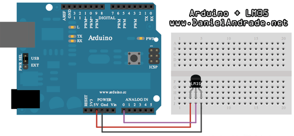
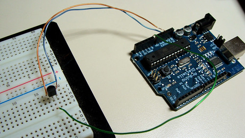
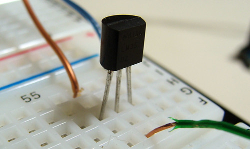
This is a quick and simple step. Just connect the 5V output from arduino to the 1st pin of the sensor, ground the 3rd pin and the 2nd one, you connect to the 0 Analog Input.
Down goes some pictures that may help you, click to enlarge:


Temperature Sensor


sens

processin


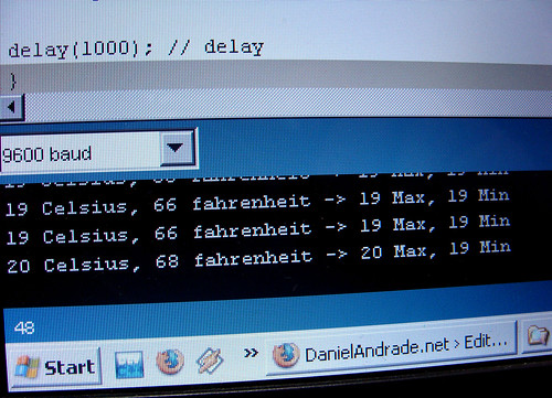
Here is the Arduino Code, just upload it and check the Serial Communication Option.
You can also download the .pde HERE.

/*
An open-source LM35DZ Temperature Sensor for Arduino. This project will be enhanced on a regular basis
(cc) by Daniel Spillere Andrade , http://www.danielandrade.net
http://creativecommons.org/license/cc-gpl
*/


int pin = 0; // analog pin
int tempc = 0,tempf=0; // temperature variables
int samples[8]; // variables to make a better precision
int maxi = -100,mini = 100; // to start max/min temperature
int i;

void setup()
{
  Serial.begin(9600); // start serial communication
}

void loop()
{
 
 
for(i = 0;i< =7;i++){ // gets 8 samples of temperature
 
  samples[i] = ( 5.0 * analogRead(pin) * 100.0) / 1024.0;
  tempc = tempc + samples[i];
  delay(1000);

}

tempc = tempc/8.0; // better precision
tempf = (tempc * 9)/ 5 + 32; // converts to fahrenheit

if(tempc > maxi) {maxi = tempc;} // set max temperature
if(tempc < mini) {mini = tempc;} // set min temperature

Serial.print(tempc,DEC);
Serial.print(" Celsius, ");

Serial.print(tempf,DEC);
Serial.print(" fahrenheit -> ");

Serial.print(maxi,DEC);
Serial.print(" Max, ");
Serial.print(mini,DEC);
Serial.println(" Min");

tempc = 0;

delay(1000); // delay before loop
}

Anything just ask!


Source by : link

Low-Cost Step-Down Converter With Wide Input Voltage Range

The circuit described here is mostly aimed at development engineers who are looking for an economical step-down converter which offers a wide input voltage range. As a rule this type of circuit employs a step-down converter with integrated switching element. However, by using a more discrete solution it is possible to reduce the total cost of the step-down converter, especially when manufacturing in quantity. The TL5001A is a low-cost PWM controller which is ideal for this project. The input voltage range for the step-down converter described here is from 8 V to 30 V, with an output voltage of 5 V and a maximum output current of 1.5 A.


When the input voltage is applied the PWM output of IC1 is enabled, taking one end of the voltage divider formed by R1 and R2 to ground potential. The current through the voltage divider will then be at most 25 mA: this value is obtained by dividing the maximum input voltage (30 V) minus the saturation voltage of the output driver (2 V) by the total resistance of the voltage divider (1.1 kΩ). T1 and T3 together form an NPN/PNP driver stage to charge the gate capacitance of P-channel MOSFET T2 as quickly as possible, and then, at the turn-off point, discharge it again.

The base-emitter junction of T3 goes into a conducting state when the PWM output is active and a voltage is dropped across R2. T3 will then also conduct from collector to emitter and the gate capacitance of T2 will be discharged down to about 800 mV. The P-channel MOSFET will then conduct from drain to source. If the open-collector output of the controller is deactivated, a negligibly small current flows through resistor R2 and the base of T1 will be raised to the input voltage level. The base-emitter junction of T1 will then conduct and the gate capacitance of T2 will be charged up to the input voltage level through the collector and emitter of T1.

The P-channel MOSFET will then no longer conduct from drain to source. This driver circuit constructed from discrete components is very fast, giving very quick switch-over times. Diodes D2 and D3 provide voltage limiting for the P-channel MOSFET, whose maximum gate-source voltage is 20 V. If the Zener voltage of diode D2 is exceeded it starts to conduct; when the forward voltage of diode D3 is also exceeded, the two diodes together clamp the gate-source voltage to approximately 19 V. The switching frequency is set at approximately 100 kHz, which gives a good compromise between efficiency and component size.

Finally, a few notes on component selection. All resistors are 1/16 W, 1 %. Apart from electrolytic C1 all the capacitors are ceramic types. For the two larger values (C2 and C5) the following are used:
  • C2 is a Murata type GRM21BR71C105KA01 ceramic capacitor, 1 µF, 16 V, X7R, 10 %;
  • C5 is a Murata type GRM32ER60J476ME20 ceramic capacitor, 47 µF, 6.3 V, X5R, 10 %. D1 (Fairchild type MBRS340T3) is a 40 V/3 A Schottky diode. Coil L1 is a Würth WE-PD power choke type 744771147, 47 µH, 2.21 A, 75 mΩ.
  • T1 (BC846) and T3 (BC856) are 60 V, 200 mA, 310 mW complementary bipolar transistors from Vishay. The TL5001AID (IC1) is a low-cost PWM controller with an open-collector output from Texas Instruments.

Simple Tremolo Effect

This tremolo effect circuit uses the XR2206 and the TCA730 IC which is designed as an electronic balance and volume regulator with frequency correction. The circuit is use full for stereo channels and it also has the ability to simulate the Lesley effect aka rotating loudspeaker effect.

 How does the tremolo effect circuit works
Balance and volume settings are done with a linear potentiometer for both channels. If this potentiometer is replaced with an AC voltage source, a periodic modulation of the input signal can be achieved. This AC voltage source comes from the function generator IC XR2206. This IC generates square, triangle and sine wave signals but for this project we use only the sine wave.

IC Tremolo effect circuit schematic

Circuit Project: DIY Tremolo Effect Circuit
The modulation voltage can be varied with P1 from 1 Hz up to 25 Hz. Resistor R3 sets the operation level of the sine wave generator. R5 and R6 set the DC voltage and the sine wave amplitude at the output. C2 is a ripple filter. The square wave output of the XR2206 drives T2 and a LED to optically display the frequency.

The modulating voltage reaches pin 13 of TCA730 via P3 and R10. This input functions as the volume control or in this case the volume modulation. The degree of the balance modulation (Lesley effect) can be varied with P2. A regulated power supply using 7815 IC is recommended. Do not use a non-stabilized power supply since the current variations would influence the modulation negatively.
Attach the 7815 IC to a good heat sink (about 10 cm2).

Variable Dc Supply Step Circuit Diagram

This is a Simple Variable Dc Supply Step Circuit Diagram. Intended as a replacement for generally poorly regulated `wall-type` ac/dc adapters, this Simple Variable Dc Supply Step Circuit Diagram offers superior performance to simple, unregulated adapters. 
Voltages of 3, 6, 9, and 12 V are available. The DPDT switch serves as a polarity-reversal switch. R2 through R6 can be replaced with a 2.5-kfl pot for a variable voltage of 1 to 12 V. R7 through RIO can be replaced by a fixed resistor of about 1 kfi if the LED1 brightness variation with output voltage is not a problem.
Simple Variable Dc Supply Step Circuit Diagram

Diode Cmos Stabilizer Circuit Diagram

The simple diode network can stabilize the voltage supplied to CMOS circuitry from a battery. D1 and D2 must have a combined forward-voltage drop of about 1.5 V. And D3 is an LED with a forward-voltage drop of about 1.7 V. The table shows the network`s output voltage as the battery`s voltage declines. [Link]
 Diode Cmos Stabilizer Circuit Diagram
Build a Diode Cmos Stabilizer Circuit Diagram

Variable DC Power Supply Circuit Diagram

This project provides the schematic & the parts list needed to construct a simple DC Power Supply from an input power supply of 7-20 V AC or 7-30V DC. This project will come in handy in case you use plenty of batteries for your basic electronics project.
Two DC voltage outputs are available; is a fixed regulated 5V for TTL use. The other output is variable from 5V upwards. The maximum output voltage depends on the input voltage. The specified maximum input DC voltage to the regulator is 35V. The maximum input voltage must be two volts higher than the regulated output voltage.
 

Variable DC Power Supply Circuit Diagram

Variable DC Power Supply (Rise)
The DC Power Supply circuit is based around the 7805 voltage regulator. It's only three connections input, output & ground & it provides a fixed output. The last digits of the part number specify the output voltage, e g. 05, 06, 08, ten, 12,15, 18, or 24. The 7800 series provides up to one amp load current & has on-chip circuitry to close down the regulator if any attempt is made to operate it outside its safe operating area.It can be seen that there's in fact separate circuits in this power supply. 7805 is directly connected as a fixed 5V regulator. The second 7805 has a resistor divider network on the output. A variable 500 ohm potentiometer is used to vary the output voltage from a maximum of 5V up to the maximum DC voltage depending on the input voltage. It will be about 2V below the input DC voltage.
The capacitor across the output improves transient response. The giant capacitor across the input is a filter capacitor to help smooth out ripple in the rectified AC voltage. The larger the filter capacitor the lower the ripple.
For tiny applications the heat sinks won't be needed. The tab on the regulator will dissipate 2W at 25 o C in air. (This is equivalent, for example, to an input voltage of 9V, an output of 5V & drawing 500 m A.) However, as your projects get bigger they will draw more current from the power supply and the regulators will operate at a higher temperature and a heat sink will be needed. You can basically add voltage & current meters to it and put it in to an appropriate plastic case connected to a transformer.
Trouble Shooting Procedure

An LED has been put in to the output of the fixed 5V regulator to indicate that the circuit is working. Poor soldering is the most likely reason that the circuit does not work. Check that all the soldering is done properly. Check that all parts are in their correct position on the PCB. Other items to check are to make sure that the regulators, electrolytic capacitor & bridge rectifier are inserted in the correct orientation.

Real Time Clock Using the PIC16CXXX

A very simple real time clock electronic project can be designed using the PIC16CXXX microcontroller family , designed by Microchip Technology . This real time clock electronic project uses the Timer1 module, from a mid-range PIC16CXXX microcontroller, to control a low-power real-time clock. Timer1 was chosen because it has its own crystal which allows the module to operate during sleep.

Upon power-up, the device is initialized with the display starting at 12:00 PM, and Timer1 is configured to generate an interrupt (every second). The Timer1 overflow interrupt wakes the device from sleep. This causes the time registers (HRS, MIN, SECS) to be updated. If the SECS register contains an even value (SECS<0> = 0), the colon (":") is not displayed. This gives a visual indication for each second. Then the device returns to sleep.

Real Time Clock Circuit Diagram

Real Time Clock Circuit Diagram

For setting the clock are used three keys : SELECT_UNITS Key (S1) selects which units are to be modified (hours, minutes, off), the INC Key (S2) increments the selected units and CLR_MIN Key (S3) clears the minutes and seconds (useful for exactly setting the time ) .

This simplify design use a standard Hitachi LCD display module and some other electronic parts .

The RA2:RA0 pins are the control signals to the LCD display, RB3:RB0 acts as a 4-bit data bus, and RB7:RB5 are the input switches. The OSC1 pin is connected to an RC network, which generates an approximate 4 MHz device frequency. Because Timer1 operates asynchronously to the device, the device's oscillator can be configured for RC mode.

Timer1’s crystal is connected to the T1OSI and T1OSO pins. A good choice for a crystal is a 32.786 kHz (watch) crystal.

This electronic project and source code was designed by Mark Palmer Microchip Technology Inc.

How to Make 12-9 Volt DC to DC Converter BD139

This circuit is a DC voltage output from a small DC input generate large voltage.It ‘s easy and quick to do, and reducing the value of the Z-diode, the circuit can be universally adapted to other output devices of the circuit voltages. The give and all diagrams represent a DC converter with 12V battery 9 volt DC input and output.
  

12-9 Volt DC to DC Converter Circuit Diagram


With the 10V zener diode, as in the diagram, the output voltage is approximately 9.3 volts DC. The supply voltage is used, should always be at least a few volts higher than the Zener voltage. In this example, I have a 12 Volt DC battery to provide regulated 9-volt DC output. Link

Simple Power LED Driver

If you want to operate power LEDS with a truly constant current which significantly prolongs the lifetime of the lamp and avoid the power loss resulting from using a constant voltage supply with a series resistor, you need a suit-able constant current source. However, the only way to achieve really good efficiency is to use a switching regulator. Altogether, this means that you need a switching regulator designed to generate a constant current instead of a constant voltage.

With this in mind, the author started working on the development of a LED pocket torch with especially high efficiency. Along with using high-capacity rechargeable batteries to maximise operating life, it’s worthwhile to be able to reduce the brightness, and therefore the operating current of the LEDs, when you don’t need full power. Accordingly, the author incorporated a dimming function in the design, based on operation in PWM mode in to reduce power losses to an absolute minimum.

Power LED Driver Circuit Diagram


Power LED Driver Circuit Diagram
As you can see from the circuit diagram, the author chose an LT3518 switching regulator IC, which is a buck/boost converter optimised for LED operation. Here it is used as a down converter (buck mode). This IC can achieve better than 90% efficiency in this mode, depending on the input voltage. According to the typical application circuit on the data sheet [1], its switching frequency can be set to approximately 170 kHz by selecting a value of 82 kΩ for R1. To maximise overall efficiency with this type of IC, the volt-age drop over the sense resistor used to measure the current flowing through the LED should be as low as possible. This particular device operates with a voltage drop of 100 mV, corresponding to a current of just under 1.5 A with the specified value of 68 mΩ for R2. This value proved to be suitable for the Cree LED used by the author. At this current level, a diode with a power rating of at least 6 W should be used for D1.

IC1 has an additional property that is ideal for this application: the connect-ed LED can be dimmed by applying a PWM signal to pin 7 of the IC, with the brightness depending on the duty cycle. Obviously, the PWM frequency must be lower than the switching frequency. The PWM signal is provided by IC2, a special voltage-controlled PWM generator (type LTC6992 [2]). The duty cycle is controlled by the volt-age applied to the MOD input on pin1 (range 0–1 V). The resistor connected to pin 3 determines the internal clock frequency of the IC according to the formula f= 1 MHz × (50 kΩ/R3). This yields a frequency of approximately 73.5 kHz with R3 set to 680 kΩ, which is much too high for controlling IC1.

However, the PWM IC has an internal frequency divider with a division factor controlled by the voltage applied to pin 4, which in this circuit is taken from voltage divider R4/R5. The division factor can be adjusted over the range of 1 to 16,384. The division factor with the specified component values is 64, resulting in a PWM frequency of around 1,150 Hz. If you want to be able to generate a PWM signal with an adjust-able duty cycle over the full range of 0 to 100%, you must use the LTC6992-1 option. The -4 option, which provides a range from 5 to 100%, might be an acceptable alternative.To prevent the duty cycle (and thus the brightness of the LED) from depending on the battery voltage, which gradually drops as the battery discharges, IC3 generates a stabilised 1.24 V control voltage for potentiometer P1. Series resistor R7 reduces the voltage over P1 to 1V, which exactly matches the input voltage range of the LTC6992.

All capacitors should preferably be ceramic types, in particular due to their low effective series resistance (ESR) as well as other favourable characteristics. However, only capacitors with X5R or X7R dielectric should be used; capacitors with type Y dielectric have very poor temperature characteristics.The supply voltage is limited to 5.5V by the maximum rated supply voltage of IC2. The author used four NiMH re-chargeable cells connected in series, which yields a voltage that is just within spec. With an operating voltage in the range of 4.5 V to 5.5 V, you must use an LED that can operate at less than 4V.

This eliminates devices with several chips connected in series on a carrier, which is very often the case with power LEDS rated at over 5 W. These devices require a correspondingly higher supply voltage, which means more cells connected in series. This is only possible if the supply voltage for IC2 is reduced by a 5 V voltage regulator or other means, and of course R4 must also be connected to this lower supply voltage.

Finally, a few words about soldering. An exposed thermal pad must be provided on the PCB for the LT3518, and the rear face of the IC must be soldered to this pad. The author obtained good results by dimensioning the exposed pad large enough to extend beyond the outline of the IC. When assembling the board, first tin the pad and the rear face of the IC. Then heat the pad with a soldering iron. When the solder melts, withdraw the tip of the soldering iron to the edge of the pad and simultaneously place the IC on the pad and align it. After this the pins can be soldered.

Author : Burkhard Kainka Copyright: Elektor

Simple Systematic Power Booster Circuit Diagram

This is a Simple Systematic Power Booster Circuit Diagram. The Power Booster solves the power distribution problem in a CATV network caused by high resistance and low energy-efficient. This power booster functions as a high-efficiency `power multiplexer` or, if you supply an external signal-source, as a high-power linear amplifier. 

 Simple Systematic Power Booster Circuit Diagram

Simple Systematic Power Booster Circuit Diagram
If you want to drive a load with a high-power square wave, the circuit simply draws power from two external power sources, VI and V2, alternately. In this mode, the circuit`s power-handling devices function as switches, dissipating minimal power. The RC time constant of the integrator, IC1, determines the circuit`s oscillation period. If you supply an external drive waveform, the circuit functions as a linear amplifier, and, consequently, inherently dissipates varying portions of that power. 
The power amplifier is stable for gains > 15. Diodes D1 and D2 limit the FET`s gate-voltage swing to less than 15 V. D3 is a dual Schottky diode that protects the FETs from short circuits between the two supplies, VI and V2, through a FET`s parasitic diode. With D3 in place, you can choose either power channel for the higher voltage input, lb drive the FETs, Q5 and Q6, at switching frequencies greater than 1 kHz, you will have to use gate drivers for them.

Electronic Extended Play Circuit Diagram

This is a Electronic Extended Play Circuit Diagram. A single op amp-one of four contained in the popular LM324-is operating in a variable pulse width, free-running square wave oscillator circuit, with its timed output driving two transistors that control the on/ off cycle of the tape-drive motor. The Oscillator` s positive feedback path holds the secret to the successful operation of the variable on/ off timing signal. 

 Electronic Extended Play Circuit Diagram

The two diodes and pulse width potentiometer R8 allows the setting of the on and off time, without affecting the oscillator`s operating frequency. One diode allows only the discharge current to flow through it and the section of R8 that it`s connected to. The other diode, and its portion of R8, sets the charge time for the timing capacitor, C3. Since the recorder`s speed is controlled by the precise off/on timing of the oscillator, a simple voltage-regulator circuit (Ql, R3, and D4) is included. 
Connecting the speed control to most cassette recorders is a simple matter of digging into the recorder and disconnecting either of the· motor`s power leads, the ground or common side might be best, and connecting the recorder through a length of small, shielded ci!ble to the control circuit. In some recorders, a remote input jack is furnished to remotely tum on and off the recorder. Before going in and modifying a recorder with a remote jack, try connecting the circuit to the external remote input.

Using Cd4066B Touch Switch Circuit Diagram

Build a Using Cd4066B Touch Switch Circuit Diagram.The CD4066B consists of four bilateral switches, each with independent controls. When touch switch SI is activated, R4 is driven high, and the control voltage goes high, which latches the switch. When S2 is activated, R4 goes low and the control voltage goes low, which deactivates the switch.

Using Cd4066B Touch Switch Circuit Diagram

Using Cd4066B Touch Switch Circuit Diagram

Make Your Iphone Battery Last Longer

I’ve owned a Iphone for a while now, it’s an amazing phone, the best I have ever used so far. But when I first started using it, my only concern was that the battery didn’t last as much as I expected. After two days, it was gone, and when I needed it, the phone just didn’t turn ON. I used to let the wireless on almost all the time and downloading many new apps. Now that I have some more experience on how my little gadget works, I will try to share some ideas on how you can optimize your iphone’s battery life and have a better iExperience.

iphone


  • Wireless connectivity will drawn your battery even if you are not using it. Keeping it on, it will always try to connect to some open hot spot, try to check your emails and much more. So a good idea is to turn it on when using, and after, turn it off.
  • Bluetooth have a similar battery usage as Wi-Fi, so there’s not much reason to leave it on if you are not using it (I believe that the most common usage for bluetooth today is the headsets and car kits).
  • Auto-Brightness is a interesting thing apple made to make the battery last longer. It uses iphone’s camera to adjust brightness based on the lighting conditions outside, so it will automatically set, for example, to make it less bright when you are on a dark place. Great feature!
  • Music EQ will have a significant battery usage if you listen to your songs for many hours everyday, as it uses more processing power. So if you want to charge less your iphone, it is another thing you may consider turning it off.
  • Heat can be a problem to your iphone, as it is a very bad thing to lithium-ion batteries, making them harder to charge and destroying it due the intense ionization. So remember to never let your phone in a hot place such as inside a car or in direct sunlight. If you are using some kind of carrying case, you need to be even more careful about this, and remember to take it off when charging your mobile, as it gets warm when charging.
  • Keep it charging! After putting your phone to charge, leave it there for some hours more after it says it’s full. It will make your phone battery last much more, you will be surprised! After done that, my iphone battery lasted more then a week, way more if you compare to the 2-3 days when I was disconnecting if from the dock just after it says its full.
  • Background Programs! This is important, new iphones, such as Iphone4 allows you to run multiple apps on the background, but this will drain your battery fast if you forget to close them. To do this, double click on the round button and it will show all the apps currently running, keep clicking in one of the apps and a red “X” will apear, then you can close all apps.
  • What else do you do to make your iphone battery last longer?


    Source by : link

    Simple Solar charger circuit project using transistors

    Solar charger circuit project using transistors. A very simple solar charger circuit project can be designed using few external electronic parts . This simple solar charger circuit is capable of handling charge currents of up to 1A. Alternate component values are given in the figure for lower current applications.


    Solar charger circuit project using transistors


    12V-SLA-chargher Solar charger circuit project using transistors circuit diagram

    The only adjustment is the voltage trip point when the current is shunted through the transistor and load resistor. This should be set with a fully charged battery. As the transistor and R3 have the entire panel’s output across them when the battery is fully charged, all of the current from the panel will be going through R3 and the Darlington transistor TIP112, so these must be well heat sunk. Adjust R1 for the trip point, usually 14.4 V – 15 V for a 12 V SLA or a 12 V Ni-Cd battery.


    source : Link

    Make a Photodiode Alarm Circuit Diagram

    Make a Photodiode Alarm Circuit Diagram. This Photodiode based Alarm can be used to give a warning alarm when someone passes through a protected area. The circuit is kept standby through a laser beam or IR beam focused on to the Photodiode. When the beam path breaks, alarm will be triggered.

    The circuit uses a PN Photodiode in the reverse bias mode to detect light intensity. In the presence of Laser / IR rays, the Photodiode conducts and provides base bias to T1. The NPN transistor T1 conducts and takes the reset pin 4 of IC1 to ground potential. IC1 is wired as an Astable oscillator using the components R3, VR1 and C3. The Astable operates only when its resent pin becomes high. When the Laser / IR beam breaks, current thorough the Photodiode ceases and T1 turns off. The collector voltage of T1 then goes high and enables IC1. The output pulses from IC1 drives the speaker and alarm tone will be generated.

    Make a Photodiode Alarm Circuit Diagram
    Circuit Project: Photodiode Alarm circuit
    IR Transmitter Circuit
    Circuit Project: Photodiode Alarm circuit
    A simple IR transmitter circuit is given which uses Continuous IR rays. The transmitter can emit IR rays up to 5 meters if the IR LEDs are enclosed in black tubes. Link

    Balanced Microphone Amplifier

    We published a design for a stereo microphone preamplifier with balanced inputs and a phantom power supply. The heart of this circuit was a special Analog Devices IC, the SSM2017. Unfortunately, this IC has been discontinued. In its place, the company recommends using the pin-compatible AMP02 from its current product line. However, and again unfortunately, the specifications of this opamp make it considerably less suitable for use as a microphone amplifier. By contrast, Texas Instruments (in their Burr Brown product line) offer an integrated instrumentation amplifier (type 1NA217) that has better specifications for this purpose.


    Incidentally, this IC is also recommended as a replacement for the SSM2017. It features internal current feedback, which ensures low distortion (THD + noise is 0.004 % at a gain of 100), low input-stage noise (1.3 nV/√Hz) and wide bandwidth (800 kHz at a gain of 100). The supply voltage range is ±4.5 V to ±18 V. The maximum current consumption of the 1NA217 is ±12 mA. The gain is determined by only one resistance, which is the resistance between pins 1 and 8 of the IC. The circuit shown here is a standard application circuit for this instrumentation amplifier. R1 and R2 provide a separate phantom supply for the microphone connected to the amplifier (this is primarily used with professional equipment).

    Balanced Microphone Amplifier Circuit Diagram
    Balanced Microphone Amplifier Circuit Diagram

    This supply can be enabled or disabled using S1. C1 and C2 prevent the phantom voltage from appearing at the inputs of the amplifier. If a phantom supply is not used, R1 and R2 can be omitted, and it is then better to use MKT types for C1 and C2. Diodes D1–D4 are included to protect the inputs of the 1NA217 against high input voltages (such as may occur when the phantom supply is switched on). R4 and R5 hold the bias voltage of the input stage at ground potential. The gain is made variable by including potentiometer P1 in series with R6. A special reverse log-taper audio potentiometer is recommended for P1 to allow the volume adjustment to follow a linear dB scale.

    The input bias currents (12 µA maximum!) produce an offset voltage across the input resistors (R4 and R5). Depending on the gain, this can lead to a rather large offset voltage at the output (several volts). If you want to avoid using a decoupling capacitor at the output, an active offset compensation circuit provides a solution. In this circuit, a FET-input opamp with a low input offset (an OPA137) is used for this purpose. It acts as an integrator that provides reverse feedback to pin 5, so the DC output level is always held to 0 V. This opamp is not in the audio signal path, so it does not affect signal quality. Naturally, other types of low-offset opamps could also be used for this purpose. The current consumption of the circuit is primarily determined by the quiescent current of IC1, since the OPA137 consumes only 0.22 mA.


    Author: T. Giesberts
    Copyright: Elektor Electronics

    Simple LCD Module in 4-bit Mode

    In many projects use is made of alphanumeric LCDs that are driven internally by Hitachi’s industry-standard HD44780 controller. These displays can be driven either in 4-bit or 8-bit mode. In the first case only the high nibble (D4 to D7) of the display’s data bus is used. The four unused connections still deserve some closer attention. The data lines can be used as either inputs or outputs for the display. It is well known that an unloaded output is fine, but that a floating high-impedance input can cause problems. So what should you do with the four unused data lines when the display is used in 4-bit mode? This question arose when a circuit was submitted to us where D0-D3 where tied directly to GND (the same applies if it was to +5 V) to stop the problem of floating inputs.

    The LCD module was driven directly by a microcontroller, which was on a development board for testing various programs and I/O functions. There was a switch present for turning off the enable of the display when it wasn’t being used, but this could be forgotten during some experiments. When the R/Wline of the display is permanently tied to GND (data only goes from the microcontroller to the display) then the remaining lines can safely be connected to the supply (+ve or GND). In this application however, the R/Wline was also controlled by the microcontroller. When the display is initialised correctly then nothing much should go wrong. The data sheet for the HD44780 is not very clear as to what happens with the low nibble during initialisation.


    After the power-on reset the display will always be in 8-bit mode. A simple experiment (see the accompanying circuit) reveals that it is safer to use pull-down resistors to GND for the four low data lines. The data lines of the display are configured as outputs in this circuit (R/Wis high) and the ‘enable’ is toggled (which can still happen, even though it is not the intention to communicate with the display). Note that in practice the RS line will also be driven by an I/O pin, and in our circuit the R/W line as well. All data lines become high and it’s not certain if (and if so, for how long) the display can survive with four shorted data lines. The moral of the story is: in 4-bit mode you should always tie D0-D3 via resistors to ground or positive.


    Author: L. Lemmens
    Copyright: Elektor Electronics

    Simple Purpose Alarm Circuit Diagram

    Simple Purpose Alarm Circuit Diagram. The alarm may be used for a variety of applications, such as frost monitor, room temperature monitor, and so on. In the quiescent state, the circuit draws a current of only a few microamperes, so that, in theory at least, a 9 V dry battery (PP3, 6AM6, MN1604, 6LR61) should last for up to ten years. Such a tiny current is not possible when ICs are used, and the circuit is therefore a discrete design. Every four seconds a measuring bridge, which actuates a Schmitt trigger, is switched on for 150 ms by a clock generator. In that period of 150 ms, the resistance of an NTC thermistor, R11, is compared with that of a fixed resistor. If the former is less than the latter, the alarm is set off.

    When the circuit is switched on, capacitor C1 is not charged and transistors T1–T3 are off. After switch-on, C1 is charged gradually via R1, R7, and R8, until the base voltage of T1 exceeds the threshold bias. Transistor T1 then comes on and causes T2 and T3 to conduct also. Thereupon, C1 is charged via current source T1-T2-D1, until the current from the source becomes smaller than that flowing through R3 and T3 (about 3 µA). This results in T1 switching off, so that, owing to the coupling with C1, the entire circuit is disabled. Capacitor C1 is (almost) fully charged, so that the anode potential of D1 drops well below 0 V. Only when C1 is charged again can a new cycle begin.

     Simple Purpose Alarm Circuit Diagram


    Simple Purpose Alarm Circuit Diagram


    It is obvious that the larger part of the current is used for charging C1. Gate IC1a functions as impedance inverter and feedback stage, and regularly switches on measurement bridge R9–R12-C2-P1 briefly. The bridge is terminated in a differential amplifier, which, in spite of the tiny current (and the consequent small transconductance of the transistors) provides a large amplification and, therefore, a high sensitivity. Resistors R13 and R15 provide through a kind of hysteresis a Schmitt trigger input for the differential amplifier, which results in unambiguous and fast measurement results. Capacitor C2 compensates for the capacitive effect of long cables between sensor and circuit and so prevents false alarms.

    If the sensor (R11) is built in the same enclosure as the remainder of the circuit (as, for instance, in a room temperature monitor), C2 and R13 may be omitted. In that case,C3 willabsorb any interference signals and so prevent false alarms. To prevent any residual charge in C3 causing a false alarm when the bridge is in equilibrium, the capacitor is discharged rapidly via D2 when this happens. Gates IC1c and IC1d form an oscillator to drive the buzzer (an a.c. type). Owing to the very high impedance of the clock, an epoxy resin (not pertinax) board must be used for building the alarm. For the same reason, C1 should be a type with very low leakage current. If operation of the alarm is required when the resistance of R11 is higher than that of the fixed resistor, reverse the connections of the elements of the bridge and thus effectively the inverting and non-inverting inputs of the differential amplifier.

    An NTC thermistor such as R11 has a resistance at –18 °C that is about ten times as high as that at room temperature. It is, therefore, advisable, if not a must, when precise operation is required, to consult the data sheet of the device or take a number of test readings. For the present circuit, the resistance at –18 °C must be 300–400 kΩ. The value of R12 should be the same. Preset P1 provides fine adjustment of the response threshold. Note that although the prototype uses an NTC thermistor, a different kind of sensor may also be used, provided its electrical specification is known and suits the present circuit.


    Author: K. Syttkus
    Copyright: Elektor Electronics


    ◄ Newer Post Older Post ►
    eXTReMe Tracker
     

    Copyright 2011 Diagram Digital Schematic is proudly powered by blogger.com