Showing posts with label Converter. Show all posts

Analog to Digital Converter Circuit Diagram

This is a digital Analog to Digital Converter Circuit Diagram. Perhaps the most important consideration of an ADC is its resolution. Because the CS5501 16-bit-delta-sigma analog-to-digital converter lacks a start convert command, it converts continuously, outputting conversion words to its output register every 1024 cycles of its master clock. However, by incorporating a standard dual J-K flip-flop into the circuit, the ADC can be configured to output a single-conversion word only when it is polled.

 Analog to Digital Converter Circuit Diagram


Analog to Digital Converter Circuit Diagram


The CS5501 converter can be operated in its asynchronous communication mode (UART) to transmit one 16-bit conversion word when it is polled over an RS-232 serial line (see figure). A null character (all zeros) is transmitted to the circuit and sets the flip-flop PF2. The CS5501 can then output a single-conversion word, which is transmitted over the RS-232 line as two bytes with start and stop bits.

The baud rate can be chosen by selecting the appropriate clock divider rate on the 74HC4040 counter/divider as the serial port clock (SLCK) for the ADC. This type of polled-mode operation is also useful when the ADC`s output register is configured to operate in the synchronous-serial clock (SSC) mode. In this case, the converter will load one output word into a 16-bit serial-to-parallel register (two 74HC595 8-bit registers) when polled to do so (see figure).

Simple Analog-to-Digital Converter with LT1018

This is a Simple Analog-to-Digital Converter with LT1018. An analog-to-digital converter (abbreviated ADC, A/D or A to D) is a device that converts a continuous physical quantity (usually voltage) to a digital number that represents the quantity's amplitude.The converter has a 60-ms conversion consumes 460 pA of 1's. 5 V power supply and maintains an accuracy of 10 bits on a 15 ° C in the temperature range of 35 ° C. 

 Simple Analog-to-Digital Converter with LT1018 Circuit Diagram


Simple Analog-to-Digital Converter with LT1018 Circuit Diagram


A pulse applied to convert the command line causes Q3, operating in reverse mode, the discharge path through the diode 10 kO, forcing its collector low. Q3 results of reverse mode switching in a capacitor discharge to 1 mV of ground. During the time of the ramp value is less than the input voltage, output of the CIA is low. 

This allows pulses ClB stabilized quartz oscillator, modulating Q4. The output data appears at the collector of Q4. When the ramp crosses the starting value of the output voltages of the CIA is going up, Q4 polarization and output data continuously. The number of pulses at the output is directly proportional to the input voltage. To celebrate cali apply 0.5V to the input and the TRIM-10 kO exactly 1000 pulses each time the conversion from the command line is pulsed.

Low-Cost Step-Down Converter With Wide Input Voltage Range

The circuit described here is mostly aimed at development engineers who are looking for an economical step-down converter which offers a wide input voltage range. As a rule this type of circuit employs a step-down converter with integrated switching element. However, by using a more discrete solution it is possible to reduce the total cost of the step-down converter, especially when manufacturing in quantity. The TL5001A is a low-cost PWM controller which is ideal for this project. The input voltage range for the step-down converter described here is from 8 V to 30 V, with an output voltage of 5 V and a maximum output current of 1.5 A.


When the input voltage is applied the PWM output of IC1 is enabled, taking one end of the voltage divider formed by R1 and R2 to ground potential. The current through the voltage divider will then be at most 25 mA: this value is obtained by dividing the maximum input voltage (30 V) minus the saturation voltage of the output driver (2 V) by the total resistance of the voltage divider (1.1 kΩ). T1 and T3 together form an NPN/PNP driver stage to charge the gate capacitance of P-channel MOSFET T2 as quickly as possible, and then, at the turn-off point, discharge it again.

The base-emitter junction of T3 goes into a conducting state when the PWM output is active and a voltage is dropped across R2. T3 will then also conduct from collector to emitter and the gate capacitance of T2 will be discharged down to about 800 mV. The P-channel MOSFET will then conduct from drain to source. If the open-collector output of the controller is deactivated, a negligibly small current flows through resistor R2 and the base of T1 will be raised to the input voltage level. The base-emitter junction of T1 will then conduct and the gate capacitance of T2 will be charged up to the input voltage level through the collector and emitter of T1.

The P-channel MOSFET will then no longer conduct from drain to source. This driver circuit constructed from discrete components is very fast, giving very quick switch-over times. Diodes D2 and D3 provide voltage limiting for the P-channel MOSFET, whose maximum gate-source voltage is 20 V. If the Zener voltage of diode D2 is exceeded it starts to conduct; when the forward voltage of diode D3 is also exceeded, the two diodes together clamp the gate-source voltage to approximately 19 V. The switching frequency is set at approximately 100 kHz, which gives a good compromise between efficiency and component size.

Finally, a few notes on component selection. All resistors are 1/16 W, 1 %. Apart from electrolytic C1 all the capacitors are ceramic types. For the two larger values (C2 and C5) the following are used:
  • C2 is a Murata type GRM21BR71C105KA01 ceramic capacitor, 1 µF, 16 V, X7R, 10 %;
  • C5 is a Murata type GRM32ER60J476ME20 ceramic capacitor, 47 µF, 6.3 V, X5R, 10 %. D1 (Fairchild type MBRS340T3) is a 40 V/3 A Schottky diode. Coil L1 is a Würth WE-PD power choke type 744771147, 47 µH, 2.21 A, 75 mΩ.
  • T1 (BC846) and T3 (BC856) are 60 V, 200 mA, 310 mW complementary bipolar transistors from Vishay. The TL5001AID (IC1) is a low-cost PWM controller with an open-collector output from Texas Instruments.

How to Make 12-9 Volt DC to DC Converter BD139

This circuit is a DC voltage output from a small DC input generate large voltage.It ‘s easy and quick to do, and reducing the value of the Z-diode, the circuit can be universally adapted to other output devices of the circuit voltages. The give and all diagrams represent a DC converter with 12V battery 9 volt DC input and output.
  

12-9 Volt DC to DC Converter Circuit Diagram


With the 10V zener diode, as in the diagram, the output voltage is approximately 9.3 volts DC. The supply voltage is used, should always be at least a few volts higher than the Zener voltage. In this example, I have a 12 Volt DC battery to provide regulated 9-volt DC output. Link

12V Step-Down Dc Converter Using ADP2300 ADP2301

Using ADP2300 ADP2301 step-down dc dc regulators with integrated power MOSFET, can be designed a very simple DC DC voltage converter. Output voltage delivered by these circuits can be adjusted from 0.8 volts, up to 0.85xVin , with ±2% accuracy. The maximum output current that can be provided by ADP2300 ADP2301 regulators is up to 1.2 A load current.

12V Step-Down Dc Converter Circuit Diagram

 
12V Step-Down Dc-Converter-Circuit Diagram
12V Step-Down Dc-Converter-ADP2301

There are two frequency options: the ADP2300 runs at 700 kHz, and the ADP2301 runs at 1.4 MHz. These options allow users to make decisions based on the trade-off between efficiency and total solution size. Current-mode control provides fast and stable line and load transient performance.  Bellow you an see two design examples, which require few common electronic components.First circuit will provide a 2.5V output at a maximum current of 1.2A from an input voltage of 12 volts. Second circuit will provide a 5V output at a maximum current of 1.2A from an input voltage of 12 volts.

Build a Converter : VGA to BNC Adapter

There are monitors which only have three BNC inputs and which use composite synchronization (‘sync on green’). This circuit has been designed with these types of monitor in mind. As can be seen, the circuit has been kept very simple, but it still gives a reasonable performance. The principle of operation is very straightforward. The RGB signals from the VGA connector are fed to three BNC connectors via AC-coupling capacitors. These have been added to stop any direct current from entering the VGA card. A pull-up resistor on the green output provides a DC offset, while a transistor (a BS170 MOSFET) can switch this output to ground. It is possible to get synchronisation problems when the display is extremely bright, with a maximum green component.

In this case the value of R2 should be reduced a little, but this has the side effect that the brightness noticeably decreases and the load on the graphics card increases. To keep the colour balance the same, the resistors for the other two colors (R1 en R3) have to be changed to the same value as R2. An EXOR gate from IC1 (74HC86) combines the separate V-sync and H-sync signals into a composite sync signal. Since the sync in DOS-modes is often inverted compared to the modes commonly used by Windows, the output of IC1a is inverted by IC1b. JP1 can then by used to select the correct operating mode. This jumper can be replaced by a small two-way switch, if required.

Converter : VGA to BNC Adapter Circuit Diagram


VGA to BNC adapter PCB layout

 This switch should be mounted directly onto the PCB, as any connecting wires will cause a lot of interference. The PCB has been kept as compact as possible, so the circuit can be mounted in a small metal (earthed!) enclosure. With a monitor connected the current consumption will be in the region of 30 mA. A 78L05 voltage regulator provides a stable 5 V, making it possible to use any type of mains adapter, as long as it supplies at least 9 V. Diode D2 provides protection against a reverse polarity. LED D1 indicates when the supply is present. The circuit should be powered up before connecting it to an active VGA output, as otherwise the sync signals will feed the circuit via the internal protection diodes of IC1, which can be noticed by a dimly lit LED. This is something best avoided.  

Resistors: 
R1,R2,R3 = 470Ω 
R4 = 100Ω 
R5 = 3kΩ3 

Capacitors: 
C1,C3,C5 = 47µF 25V radial 
C2,C4,C6,C7,C10 = 100nF ceramic 
C8 = 4µF7 63V radial 
C9 = 100µF 25V radial 

Semiconductors: 
D1 = LED, high-efficiency
D2 = 1N4002
T1 = BS170
IC1 = 74HC86
IC2 = 78L05

Miscellaneous:
JP1 = 3-way pinheader with jumper
K1 = 15-way VGA socket (female), PCB mount (angled pins)
K2,K3,K4 = BNC socket (female), PCB mount, 75Ω

How to build 1.5V to 5V/12V DC/DC Converter with LT1073

Small 1.5V to 5V or 12V DC/DC converter with LT1073 chip. The IC is available in three different versions, depending on output voltage. Two with fixed output voltage of 5V and 12V, and the most interesting that can be adjusted. The adjustment is done through a voltage divider with two resistors, of mass, output and Terminal 8, internally connected to the voltage comparator IC, which is responsible for stabilizing the output voltage.

1.5V to 5V/12V DC/DC Converter with LT1073

LT1073 has an internal everything you need to make a small DC / DC converter with a low operating voltage of only 95μA 1V and consumption without load.

If you do not have a meter inductance, the inductive part of the drive is a bit more complicated to make, but we shall see some possible solutions. Capacitor also recommended by the manufacturer for the circuit is a bit hard to get, I have used a tantalum recovered from another power source, and the ripple voltage at the output is quite low. Last but not least, say that the diode has to be a fast, not worth as the 1N4002 rectifiers, the 1N5818 is recommended schottky type, characterized by high response time and low internal resistance, which is what ideal for this type of converters.

As we can see from the photograph of the circuit in a low energy lamp, ay a small toroidal core can be recovered. 82μH To this core, we winding 7 turns of 0.3mm enamelled copper wire.

Another option is to use a toroidal core Ferroxcube, Farnell code 178-504 of 13.25 x7, 35x5, 7mm, grade 3C85, value AL 1000. with this core we have winding 8 turns to 90μH.

Finally, note that you can download the documentation in the manufacturer's website, is very good and complete, with numerous examples of applications, and above all very clear.

1.5V to 5V/12V DC/DC Converter with LT1073

1.5V to 5V/12V DC/DC Converter with LT1073


1.5V to 5V/12V DC/DC Converter with LT1073

1.5V to 5V/12V DC/DC Converter with LT1073 ab

Build 12V to 9V DC Converter

To get a more precise output voltage, replace zener diode Z1 with 10V and R1 with a 1Kilo ohm potentiometer. A Coolrib for Q1 is optional but highly recommended. You can replace Q1 for a more robust type to get more output amps depending on your requirements. Simple circuit to power your 9 volt cassette recorder and other stuff.


http://diagramdigital.blogspot.com/2012/11/build-12v-to-9v-dc-converter.html

Parts List:

R1 = 560 ohm
C1 = 1000uF/40V, Electrolytic
C2 = 10uF/25V, Electrolytic
C3 = 330nF, Ceramic
Z1 = 9.1V, 1watt zener
Q1 = ECG184, NTE184 

Step-Up Converter For 20 LEDs

The circuit described here is a step-up converter to drive 20 LEDs, designed to be used as a home-made ceiling night light for a child’s bedroom. This kind of night light generally consists of a chain of Christmas tree lights with 20 bulbs each consuming 1 W, for a total power of 20 W. Here, in the interests of saving power and extending operating life, we update the idea with this simple circuit using LEDs. 

Power can be obtained from an unregulated 12 V mains adaptor, as long as it can deliver at least about 330 mA.  The circuit uses a low-cost current-mode controller type UCC3800N, reconfigured into voltage mode to create a step-up converter with simple compensation. By changing the external components the circuit can easily be modified for other applications. To use a current-mode controller as a voltage-mode controller it is necessary to couple a sawtooth ramp (rising from 0 V to 0.9 V) to the CS (current sense) pin, since this pin is also an input to the internal PWM comparator.

Step-Up Converter For 20 LEDs Circuit diagram :
Step-up Converter For 20 LEDs -Circuit-Diagram
Step-up Converter For 20 LEDs Circuit Diagram

The required ramp is present on the RC pin of the IC and is reduced to the correct voltage range by the voltage divider formed by R3 and R2. The RC network formed by R4 and C6 is dimensioned to set the switching frequency at approximately 525 kHz. The comparator compares the ramp with the divided-down version of the output voltage produced by the potential divider formed by R6 and R7. Trimmer P1 allows the output voltage to be adjusted. This enables the current through the LEDs to be set to a suitable value for the devices used. The UCC3800N starts up with an input voltage of 7.2 V and switches off again if the input voltage falls below 6.9 V. The circuit is designed so that output voltages of between 20 V and 60 V can be set using P1.

This should be adequate for most cases, since the minimum and maximum specified forward voltages for white LEDs are generally between 3 V and 4.5 V. For the two parallel chains of ten LEDs in series shown here a voltage of between 30 V and 45 V will be required. The power components D1, T1 and L1 are considerably over specified here, since the circuit was originally designed for a different application that required higher power. To adjust the circuit, the potentiometer should first be set to maximum resistance and a multimeter set to a 200 mA DC current range should be inserted in series with the output to the LEDs. Power can now be applied and P1 gradually turned until a constant current of 40mA flows. The step-up converter is now adjusted correctly and ready for use.


Digital 12-Bit DAC Circuit with Variable Step Size

12-Bit Digital-to-Analog Converter (DAC) with variable step size. The step size of the converter is variable by selection of the high order data bits. The first DAC, A, has a stable reference current supplied via the 10.24 V reference IC and Rl. R2 provides bias cancellation. As shown, only the first 4 MSB inputs are used, giving a step size of 225/256 2.048/16 = 0.127 mA. 

This current supplies the reference for DAC whose step size is then 0.1275/256 = 0.498 µ. Complementary voltage outputs are available for unipolar output and using R3 - R4 = 10, Vout is ± 10.2 V approximately, with a step size (1 LSB) of approximately 5 mV. If desired an op amp can be added to the output to provide a low impedance output with bipolar output symmetrical about ground, if R5 = R6 within 0.05%.

 
Digital 12-Bit DAC Circuit with Variable Step Size

Note 
That offset null is required, and all resistors except R2 and R3 should be 1% high stability types. By using lower order address lines than illustrated for DAC A, a smaller step size (and therefore full-scale output) can be obtained. Unused high order bits can be manipulated high or low to change the relative position of the full-scale output.

Simple +12v to +9v converter Circuit Diagram


This little circuit uses a LM317 variable voltage regulator to adjust the input voltage down to +9 volt, or whatever else you need. Just a solid basic circuit without bells and whistles.

You can do with a 10uF capacitor for C1 if your battery is close to this circuit. If it is located more than 3 feet increase the value to 100uF or above. Without a coolrib it can easily handle 500mA. If you need more, or the maximum current (1.5A), then a good coolrib is required.

Trimmer potent meter R3 will vary the output voltage. Ceramic capacitor C2 improves frequency/transient response. Can be omitted if not needed for your application. If you want extra protection in case the adjust pin is short circuited, add an extra 1N4001 diode over the input and the output. Cathode to input. But normally only used if the output is way over 25V.

R1 and R3 determine the output voltage. You can adapt them for your own needs and applications.
Use the following formula: (((R1+R3)/R2)+1)*1.25=V-out which comes to: (((560+1000)/220)+1)*1.25 = 10.11V (assuming V-in is 12V).

Or vice-versa: ((V-out/1.25)-1)*R2=R1+R3 which comes to: ((9/1.25)-1)*220=1364. For 1364, you can make R1=560 and R3=1K, which will give plenty of play.


After dozens of emails I have included the above circuit. The parts with the red 'X' are added and act to boost the amperage. The NTE393 transistor can handle 25A with a sufficient coolrib.

Other power transistors, such as the TIP2955, or similar can be used also. The power transistor is used to boost the extra needed current above the maximum allowable current provided via the regulator. Current up to 1500mA(1.5A) will flow through the regulator, anything above that makes the regulator conduct and adding the extra needed current to the output load.

It is no problem stacking power transistors for even more current. Both regulator and power transistor must be mounted on an adequate heatsink, and if you intend to use lots of amps a fan would be nice too.

Cheap Cost Step Down Converter Circuit Diagram

The circuit described here is mostly aimed at development engineers who are looking for an economical step-down converter which offers a wide input volt-age range. As a rule this type of circuit employs a step-down converter with integrated switching element. However, by using a more discrete solution it is possible to reduce the total cost of the step-down converter, especially when manufacturing in quantity. The TL5001A is a low-cost PWM controller which is ideal for this project.

Low Cost Step Down Converter with Wide Input Voltage Range

Low-Cost-Step-Down-Converter-Schematic-Circuit-diagram

The input voltage range for the step-down converter described here is from 8 V to 30 V, with an output voltage of 5 V and a maximum output current of 1.5 A. 

When the input voltage is applied the PWM output of IC1 is enabled, taking one end of the voltage divider formed by R1 and R2 to ground potential. The cur-rent through the voltage divider will then be at most 25 mA: this value is obtained by dividing the maximum input voltage (30 V) minus the saturation voltage of the output driver (2 V) by the total resistance of the voltage divider (1.1 kΩ). T1 and T3 together form an NPN/PNP driver stage to charge the gate capacitance of P-channel MOSFET T2 as quickly as possible, and then, at the turn-off point, discharge it again. The base-emitter junction of T3 goes into a conducting state when the PWM output is active and a voltage is dropped across R2. T3 will then also conduct from collector to emitter and the gate capacitance of T2 will be discharged down to about 800 mV. The P-channel MOSFET will then conduct from drain to source. If the open-collector output of the controller is deactivated, a negligibly small current flows through resistor R2 and the base of T1 will be raised to the input voltage level. 

The base-emitter junction of T1 will then conduct and the gate capacitance of T2will be charged up to the input voltage level through the collector and emitter ofT1. The P-channel MOSFET will then no longer conduct from drain to source. This driver circuit constructed from discrete components is very fast, giving very quick switch-over times. 

Diodes D2 and D3 provide voltage limiting for the P-channel MOSFET, whose maximum gate-source voltage is 20 V. If the Zener voltage of diode D2 is exceeded it starts to conduct; when the forward voltage of diode D3 is also exceeded, the two diodes together clamp the gate-source voltage to approximately 19 V. The switching frequency is set at approximately 100 kHz, which gives a good compromise between efficiency and component size. 

Finally, a few notes on component selection. All resistors are 1/16 W, 1 %. Apart from electrolytic C1 all the capacitors are ceramic types. For the two larger values (C2 and C5) the following are used:
  • C2 is a Murata type GRM21BR71C105KA01 ceramic capacitor, 1 µF, 16 V, X7R, 10 %;.
  • C5 is a Murata type GRM32ER60J476ME20 ceramic capacitor, 47 µF, 6.3 V, X5R, 10 %.
  • D1 (Fairchild type MBRS340T3) is a 40 V/3 A Schottky diode. Coil L1 is a Würth WE-PD power choke type 744771147, 47 µH, 2.21 A, 75 mΩ.
  • T1 (BC846) and T3 (BC856) are 60 V, 200 mA, 310 mW complementary bipolar transistors from Vishay.
  • The TL5001AID (IC1) is a low-cost PWM controller with an open-collector output from Texas Instruments. Source by Link

Vlf Converter Circuit Diagram

This converter uses a low-pass filter instead of the usual tuned circuit so the only tuning required is with the receiver. The dual-gate MOSFET and FET used in the mixer and oscillator aren`t critical. Any crystal having a frequency compatible with the receiver tuning range may be used. 

For example, with a 3500 kHz crystal, 3500 kHz on the receiver dial corresponds to zero kHz; 3600 to 100 kHz; 3700 to 200 kHz, etc (At 3500 khz on the receiver all one can hear is the converter oscillator, and VLF signals start to come in about 20 kHz higher).


VLF Converter Circuit Diagram

Vlf Converter Circuit Diagram

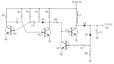
6V to 12V Converter Circuit Diagram

This inverter circuit can provide up to 800mA of 12V power from a 6V supply. For example, you could run 12V car accessories in a 6V (British?) car. The circuit is simple, about 75% efficient and quite useful. By changing just a few components, you can also modify it for different voltages.

 6V to 12V Converter Circuit Diagram

6V to 12V Converter Circuit Diagram


Parts
R1, R4 2.2K 1/4W Resistor
R2, R3 4.7K 1/4W Resistor
R5 1K 1/4W Resistor
R6 1.5K 1/4W Resistor
R7 33K 1/4W Resistor
R8 10K 1/4W Resistor
C1,C2 0.1uF Ceramic Disc Capacitor
C3 470uF 25V Electrolytic Capcitor
D1 1N914 Diode
D21N4004 Diode
D3 12V 400mW Zener Diode
Q1, Q2, Q4 BC547 NPN Transistor
Q3 BD679 NPN Transistor
L1 See Notes
MISC Heatsink For Q3, Binding Posts (For Input/Output), Wire, Board


Notes
1. L1 is a custom inductor wound with about 80 turns of 0.5mm magnet wire around a toroidal core with a 40mm outside diameter.
2. Different values of D3 can be used to get different output voltages from about 0.6V to around 30V. Note that at higher voltages the circuit might not perform as well and may not produce as much current. You may also need to use a larger C3 for higher voltages and/or higher currents.
3. You can use a larger value for C3 to provide better filtering.
4. The circuit will require about 2A from the 6V supply to provide the full 800mA at 12V.
Older Post ►
eXTReMe Tracker
 

Copyright 2011 Diagram Digital Schematic is proudly powered by blogger.com