Showing posts with label Inverters. Show all posts

Mini Power Inverter

Even robot systems occasionally need a negative supply voltage for some purpose or other, and in this kind of application in particular there is a need for an effective circuit that does  not  make  greater demands  then  necessary in terms of current or space. If a low current 5 V supply is needed and only +5 V is available, a natural manufacturer to turn  to  is  Maxim,  and indeed in this case they do not let us down.The best known integrated  circuit made by this company is the MAX232, a level shifter for serial ports with an integrated charge pump that does not need an external inductor. 

Mini Power Inverter Project  image:

 
Mini Power Inverter Img
Simple Mini Power Inverter   

Along the same lines, although with a more stable output voltage and higher efficiency, is the MAX660. The device can ‘mirror’ any input voltage between 1.5 V and 5.5 V. With a 5 V input the output is typically –4.7 V with a load of 100 mA. Efficiency at 10 mA is around 96 % and at 100 mA is around 88 %. With an open-circuit output the IC draws a quiescent current of just 120 μA.There is little to say about the circuit itself. 

Mini Power Inverter Circuit diagram :
Simple Mini Power Inverter Circuit Diagram
 
The 0 Ω resistor on pin 1 selects the operating frequency. With R1 fitted, the circuit operates at 80 kHz; without it, at 10 kHz. The combination of L1 and C5 slightly reduces ripple on the output voltage; the choice of inductor is not as critical as it would be if it formed part of the switching circuit.Gerber files for the printed circuit board (which uses some SMD components) are available for download from the Elektor website, ref. 070279-11.zip. R1, C1 and C4 are 0603 SMDs and C3 is an SMD tantalum electrolytic capacitor. Either the MAX-660CSA or the MAX660M can be used; both come in SO8 packages. L1 is a 10 μH SMD inductor rated at 300 mA. 

Soldering Iron Inverter Circuit

Here is a simple but inexpensive inverter for using a small soldering iron (25W, 35W, etc) In the absence of mains supply. It uses eight transistors and a few resistors and capacitors. Transistors Q1 and Q2 (each BC547) form an astable multivibrator that produces 50Hz signal. The complementary outputs from the collectors of transistors Q1 and Q2 are fed to pnp Darlington driver stages formed by transistor pairs Q3-Q5 and Q4-Q6 (utilising BC558 and BD140). The outputs from the drivers are fed to transistors Q7 and Q8 (each 2N3055) connected for push-pull operation.  Use suitable heat-sinks for transistors Q5 through Q8. A 230V AC primary to 12V-0-12V, 4.5A secondary transformer (T1) is used.


Soldering Iron Inverter Circuit Diagram


Soldering Iron Inverter Circuit

The centre-tapped terminal of the secondary of the transformer is connected to the battery (12V, 7Ah), while the other two terminals of the secondary are connected to the collectors of power transistors T7 and T8, respectively. When you power the circuit using switch S1, transformer X1 produces 230V AC at its primary terminal. This voltage can be used to heat your soldering iron. Assemble the circuit on a generalpurpose PCB and house in a suitable cabinet. Connect the battery and transformer with suitable current-carrying wires. On the front panel of the box, fit power switch S1 and a 3-pin socket for connecting the soldering iron. Note that the ratings of the battery, transistors T7 and T8, and transformer may vary as these all depend on the load (soldering iron).


Author : Sanjay Kumar

USB 5V to 12V DC-DC Step-Up Converter by LT1618

This is a 5V to 12V DC-DC step-up (boost) converter circuitry that is especially ideal for the USB powered applications. First of all a USB port has two current supply modes. Before detecting the connected device, it supplies maximum 100mA to the load. After recognizing the device, it increases the output current up to 500mA. In this circuit, controller (LT1618) also provides two input current modes. 100mA and 500mA input modes can be selected by the user.

USB 5V to 12V DC-DC Step-Up Converter by LT1618 


USB 5V to 12V DC-DC Step-Up Converter by LT1618

Output currents are limited due to the increased potential difference at the output. When the demand of the load increases, output voltage will start to decrease. For example, if the circuit operates in the 100 mA input mode, when the load is 35 mA, the output voltage will be kept at 12V. But if the load increases to 50 mA, output voltage will reduce to 8V to maintain the constant 100 mA input current.

Simple Inverter Window Comparator Circuit Diagram

This is a simple Inverter Window Comparator Circuit Diagram ICl-c functions as a non inverting comparator, and ICl-a operates as an inverting comparator. Potentiometer Rl and fixed resistors R2 and R3 form a divider chain that delivers slightly different voltages to the two comparators. These voltages define the upper and lower limits of the circuit`s switching window, which can be changed easily by varying R2 and R3. The LED glows only when the input voltage falls within the window region. 

Inverter Window Comparator Circuit Diagram

Inverter Window Comparator Circuit Diagram


Sourced By: Circuitsstream

Voltage Inverter using IC NE 555

In many circuits we need to generate an internal adjustable voltage. This circuit shows how it is possible to use a trusty old NE555 timer IC and a bit of external circuitry to create a voltage inverter and doubler. The input voltage to be doubled is fed in at connector K1. To generate the stepped-up output at connector K2 the timer IC drives a two-stage inverting charge pump circuit.

The NE555 is configured as an astable multivibrator and produces a rectangular wave at its output, with variable mark-space ratio and variable frequency. This results in timing capacitor C3 (see circuit diagram) being alternately charged and discharged; the voltage at pin 2 (THR) of the NE555 swings between one-third of the supply voltage and two-thirds of the supply voltage.


Voltage Inverter Circuit Using IC NE555 


The output of the NE555 is connected to two voltage inverters. The first inverter comprises C1, C2, D1 and D2. These components convert the rectangular wave signal into a nega-tive DC level at the upper pin of K2. The second inverter, comprising C4, C5, D3 and D4, is also driven from the output of IC1, but uses the negative output voltage present on diode D3 as its reference potential. The consequence is that at the lower pin of output connector K2 we obtain a negative volt-age double that on the upper pin.


Now let us look at the voltage feedback arrangement, which lets us adjust this doubled negative output voltage down to the level we want. The NE555 has a control voltage input on pin 5 (CV). Normally the voltage level on this pin is maintained at two-thirds of the supply voltage by internal circuitry. The voltage provides a reference for one of the comparators inside the device. If the reference voltage on the CV pin is raised towards the supply voltage by an external circuit, the timing capacitor C3 in the astable multivibrator will take longer to charge and to discharge. As a result the frequency of the rectangle wave output from IC1 will fall, and its mark-space ratio will also fall.

The source for the CV reference voltage in this circuit is the base-emitter junction of PNP transistor T1. If the base volt-age of T1 is approximately 500 mV lower than its emitter voltage, T1 will start to conduct and thus pull the voltage on the CV pin towards the positive supply.

In the feedback path NPN transistor T2 has the function of a voltage level shifter, being wired in common-base configuration. The threshold is set by the resistance of the feedback chain comprising resistor R3 and potentiometer P1. When the emitter voltage of transistor T2 is more than approximately 500 mV lower than its base voltage it will start to conduct. Its collector then acts as a current sink. Potentiometer P1 can be used to adjust the sensitivity of the negative feedback circuit and hence the final output voltage level.Using T1 as a voltage reference means that the circuit will adjust itself to compensate not only for changes in load at K2, but also for changes in the input supply voltage. If K2 is disconnected from the load the desired output voltage will be maintained, with the oscillation frequency falling to around 150 Hz.

A particular feature of this circuit is the somewhat unconventional way that the NE555’s discharge pin (pin 7) is connected to its output (pin 3). To understand how this trick works we need to inspect the innards of the IC. Both pins are outputs, driven by internal transistors with bases both connected (via separate base resistors) to the emitter of a further transistor. The collectors of the output transistors are thus isolated from one another [1].

The external wiring connecting pins 3 and 7 together means that the two transistors are operating in parallel: this roughly doubles the current that can be switched to ground.The two oscilloscope traces show how the output voltage behaves under different circumstances. The left-hand figure shows the behaviour of the circuit with an input voltage of 9 V and a resistive load of 470 Ω connected to the lower pin of output connector K2. The figure on the right shows the situation with an input voltage of 10 V and a load of 1 kΩ on the lower pin of output connector K2. The pulse width and frequency of the rectangle wave at the output of IC1 are automatically adjusted to compensate for the differing conditions by the feedback mechanism built around T1 and T2.

Because of the voltage drops across the Darlington out-put stage in the IC (2.5 V maximum) and the four diodes (700 mV each) the circuit achieves an efficiency at full load (470 Ω between the output and ground) of approximately 50 %; at lower loads (1 kΩ) the efficiency is about 65 %.

Author : Peter Krueger -  Copyright : Elektor

Inverter 5000 Watt PWM Circuit Diagram

This is a simple Inverter 5000 Watt PWM Circuit Diagram. This inverter uses PWM (Pulse Width Modulator) with type IC SG3524. IC serves as a oscillator 50Hz, as a regulator of the desired output voltage. Input power ranging from 250W up to 5000W output and has. Following a series INVERTER 5000W with PWM (Pulse Width Modulator).

 Inverter 5000 Watt PWM Circuit Diagram


Pcb Layout


Below is the output power settings that can be issued by this inverter:

DC voltage and Transformer "T2" winding recommendation:

Winding Power Supply

12VDC 750W P: 24V "12-0-12" / S: 220V

1500W 24VDC P: 48V "24-0-24" / S: 220V

2250w 36VDC P: 72V "36-0-36" / S: 220V

3000w 48VDC P: 96V "48-0-48" / S: 220V

3750w 60VDC P: 120V "60-0-60" / S: 220V

4500w 72VDC P: 144V "72-0-72" / S: 220V

5250w 84VDC P: 168V "84-0-84" / S: 220V


Transformer used is the transformer CT

R1 serves to regulate the voltage to 220v inverter

R2 serves to regulate the inverter output frequency of 50 or 60 Hz (as appropriate)

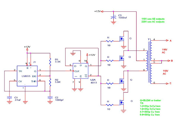
110V-220V 500W or more inverter Circuit Diagram

110V-220V 500W or more inverter Circuit Diagram

i have constructed this inverter to charge my EV
i have 12V DC from solar pannels and i need to recharge my 120V battery pack so i needed an voltage inverter
after buying one i have tested it and it blowed in 2 hours
so i started building one myself using the ferite transformer and rewired it for my use
is very sinple and can be made for every one needs
can output any AC voltage with proper wiring
i use it only with 110v for my needs but in the diagram i had added another wiring for 110 and 120V

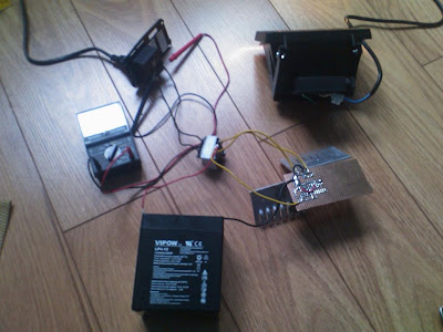
as you can see it powers an 200W halogen lamp for testing
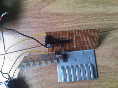
in test i have used only 2 FETS but they are too hot so i have added another 2 for more power
if you use only 250W you can use only 2 with propper cooling
if you want more that 500W you need to add another 2 for every 250W of power and use an bigger transformer

from my findings this inverter has around 75% performance

Be carefull at output you have dangerous voltage

Step 1: The built inverter for 250W

110V-220V 500W or more inverter Circuit Diagram

110V-220V 500W or more inverter Circuit Diagram


As i said this one gets hotter with an 200W halogen lamp
if you want more power use more FETs and better transformer


DO NOT TRY MORE THAN 1000W is insane
for 250W you use 310W/12V=around 25A
for 500W you use 620W/12V=around 50A
for 750W you use 930W/12V=around 75A
for 1000W you use 1240W/12V=around 100A


Step 2:

DSC_0034.jpg
DSC_0032.jpg
DSC_0048.jpgDSC_0050.jpg

You can use an inverter to power your laptop from car batetry or use any house object that uses AC curent

This is the test inverter finished

I will post more pictures after i finish mounting it in its casing for car mounting

I have 240W solar panel on the roof of my car so i can charge my car any were is i have enough time

for DC you need to add an AC/DC rectifier and you can charge your EV battery ;)


BE CAREFUL YOU ARE PLAYING WITH DANGEROUS VOLTAGE

1000W DC-AC Pure Sine Wave Power Inverter Circuit Diagram


DC-DC step-up part of the circuit RU190N08


Power circuit board


SPWM drive plate TDS2285 IC

Simple 12 to 120 Volt Inverter Circuit Diagram

This is the simple 12 to 120 Volt Inverter Circuit Diagram. Ever needed a low power 120volt AC power source for your car, van or truck? Well this circuit should do the trick for you. It will supply 15 watts of AC power to a device. It should power lamps, shavers, small stereos and small appliances. If you draw to much power the circuit will shut down all by itself. 

The output of this circuit is a square wave so there may be some noticeable hum on audio units plugged into it. To reduce some of the hum increase the value of the output capacitor which is at .47uf now. That transistor in the circuit are high power PNP transistors. Radio Shack part number 276-2025 are good ones to use or TIP32. The transformer is a 24 volt 2 amp center tapped secondary Radio Shack part number 273-1512 or equivalent. 

 12 to 120 Volt Inverter Circuit Diagram

12 to 120 Volt Inverter Circuit Diagram

Toggle Touch Switch with Two Inverter Gates

Toggle Touch Switch with Two Inverter Gates
You can make a Toggle Touch Switch with Two Inverter Gates, two resistors, and two capacitors. The schematic diagram of the circuit is shown in the figure below. At power up, the output (of U1A) will be high, and the inverting output will be low because U1A gate will be triggered to ground level by C2. After triggered, the low level of U1A input is maintained by U1B output via R2.


If we touch the pad at this condition, where the output is high, then the U1A input will go high because we “short” the voltage of C1 to the input pin, and the low level previously caused by low level of U1B output voltage connected via R2 can’t be maintained because our skin resistance is much lower than 10M.

After U1A input goes high then U1A output will go low, and now U1B will go high to maintain high voltage level of U1A via R2, so we can release our finger without loosing the last state. Touching the pad again after we release our previous touching will toggle the output as the condition is reversed.

After we touch the pad, we have to release before 1 second (R2C2 time constant) elapsed. If we touch the pad longer than R2C2 time constant then  the output will oscillate (about 1 Hz).
Older Post ►
eXTReMe Tracker
 

Copyright 2011 Diagram Digital Schematic is proudly powered by blogger.com